Zdenduino - My Own ESP32 Devboard - Part 1
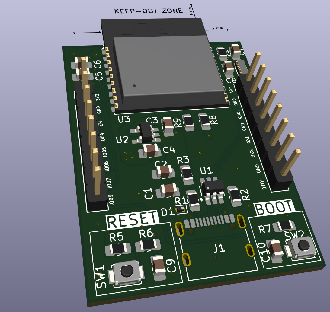
The Embedded Rite of Passage
I believe creating your own development board is one of those mandatory steps on every embedded journey. It’s the bridge between using pre-made modules and eventually designing your own Single Board Computer (SBC).
While browsing YouTube, I stumbled upon an amazing video by PajoPCB. He walks through the creation of a compact ESP32-C3 based dev board in excruciating detail. I took it as a “create-along” challenge, and it turned into a perfect weekend project.
Learning from the Master
Pajo explained everything — and I mean everything. I finally got a deep dive into:
- Impedance matching and trace differential pairing (essential for USB and RF).
- Why creating traces too thick isn’t always a good idea looking at my Connect Game traces… oops, but hey, it worked!.
- The correct usage of decoupling capacitors and ESD protection.
It was a total gold mine of practical advice.
My Design: The 2-Layer Deviation
While Pajo went for a 4-layer design, I decided to stick to a 2-layer PCB. This meant making some concessions, especially around the crystal oscillator and trace shapes.
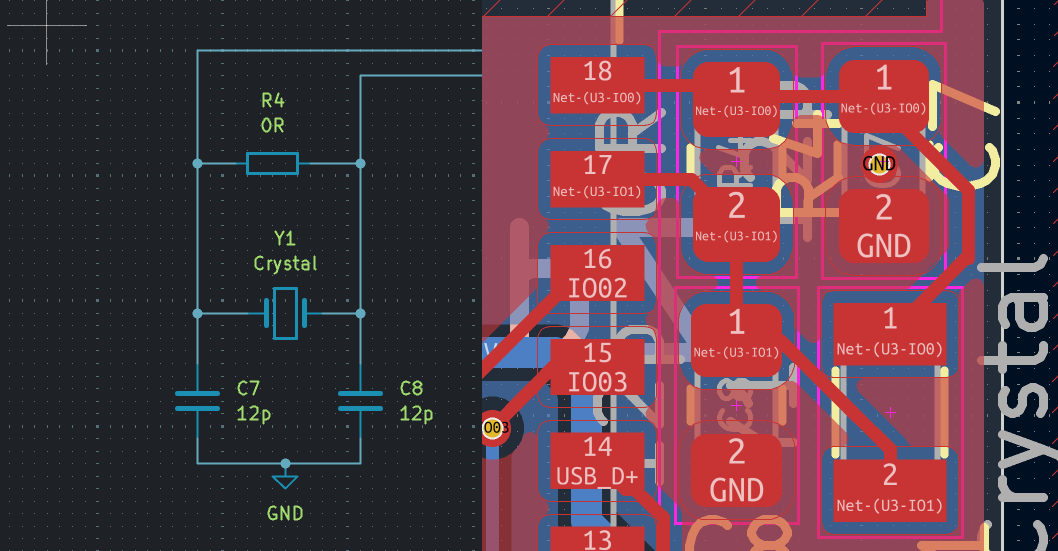
Ideally, traces for the crystal should be as short and straight as possible. I couldn’t perfectly achieve that because I set a personal goal: all components must be on one side of the PCB. It should be fine for this revision, but for high-sensitivity RF work, I’d do it differently next time.
The final result? A tiny 31x42mm PCB. Quite a jump from the 100x100mm “airfields” I used to design!
The Manufacturing Drama (JLCPCB)
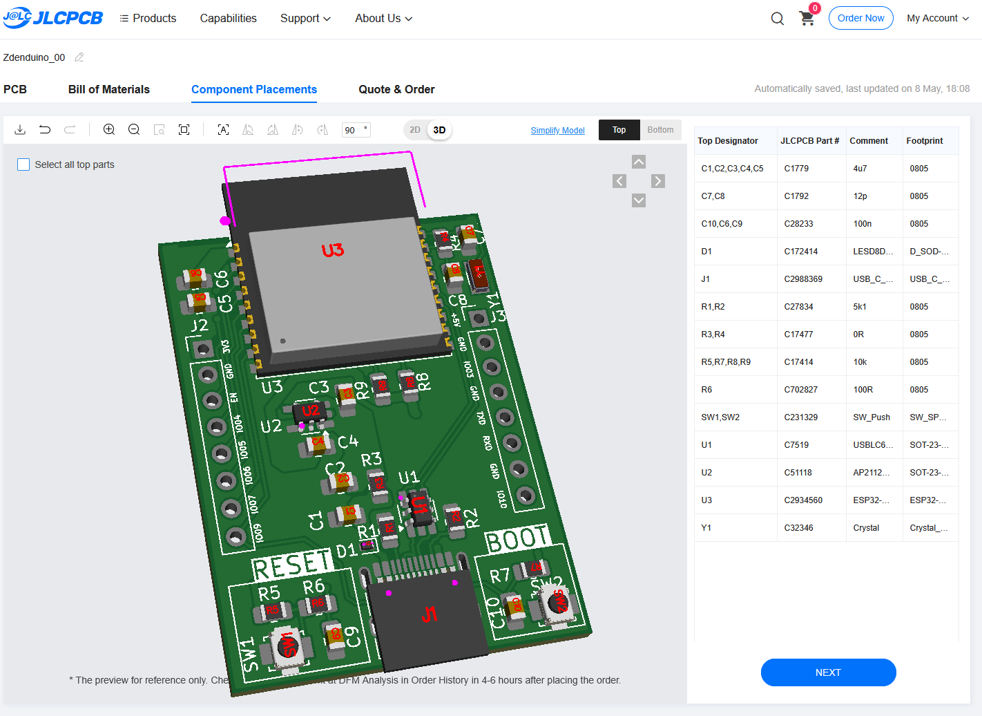
After finishing the design, I sent it off to JLCPCB. This time, I didn’t just want the boards; I wanted Full Assembly (PCBA). And boy, did things go sideways at first.
Before we dive into the errors, a quick shoutout: Use the Fabrication Toolkit plugin for KiCad! (Get it here). Without it, I would have probably given up on generating all the placement files. It’s available directly in the KiCad Plugin Manager.
The V-Cut Trap
My first design included V-cuts (panelization), thinking I was doing them a favor. Wrong. V-cuts are part of their “Standard” service, not the “Economic” one I wanted. After some back-and-forth emails, we decided to scrap the order and start over.
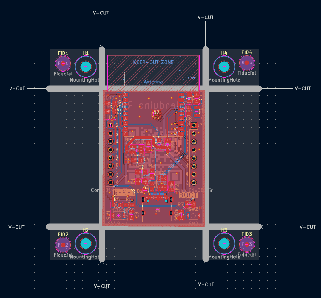
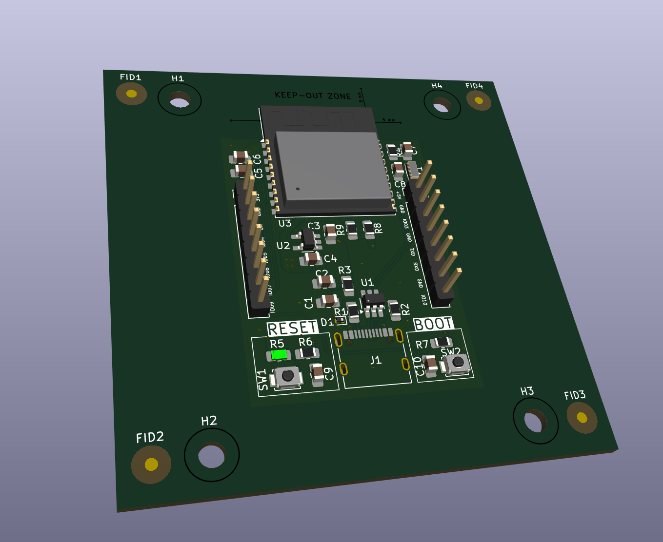
This actually worked in my favor! I had originally chosen a diode that they only had 2 pieces of in stock. In the second attempt, I swapped it for a different one with the same package (shoutout to my previous ESD diode research!).
The 50 Euro Surprise
Here is the shocker:
- My first order (2 assembled PCBs + 3 empty) was 52 Euros including customs and shipping.
- My second order (All 5 PCBs fully assembled, no V-cuts) came to… 50 Euros.
Absolutely amazing. Getting 5 fully finished boards for less than 2 is the kind of math I like.
What’s Next?
Now, we play the waiting game again. Once the boards arrive, we’ll see if my 2-layer crystal layout actually works or if I’ve created a very expensive brick.
Stay tuned for Part 2!