e-Dice - Rolling the Silicon with ATtiny1616 and LIS3DH - Part 1
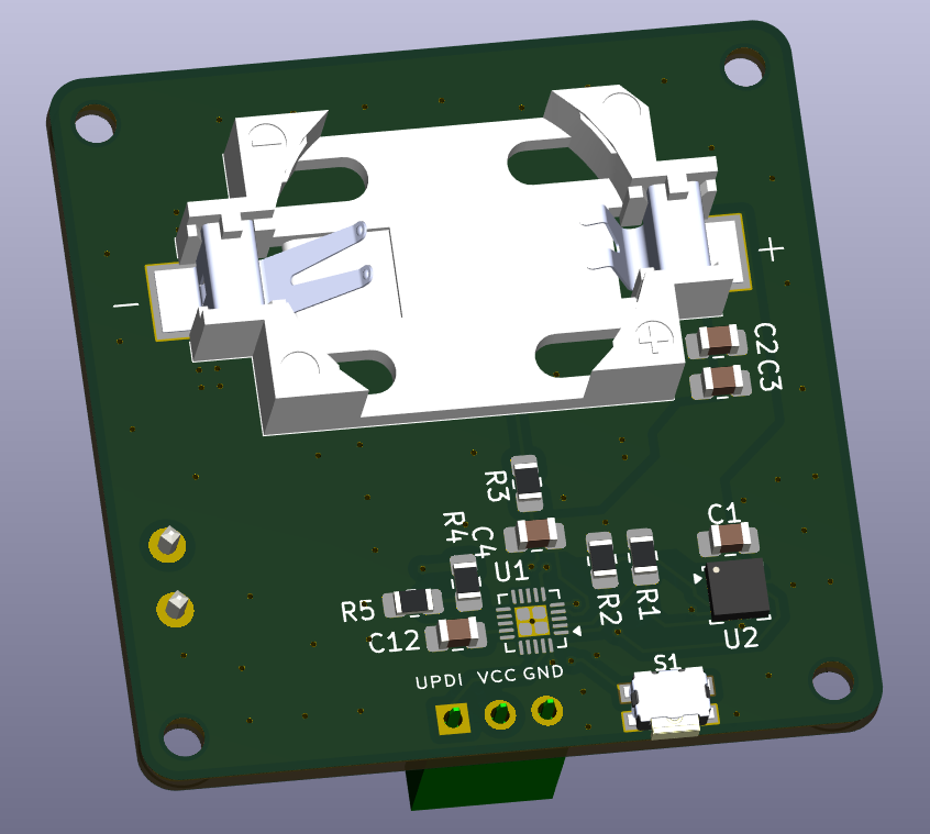
A few days ago I saw a simple pcb on my colleagues (L.Ch.) desk. A simple electronic toy, a dice with LEDs. It got me thinking “Can I do something like this? It shouldn’t be that hard” and would be nice, interactive exercise.
That was the start of project “e-Dice”. The goals are:
- 6d dice
- cyberpunk-ish estetic
- battery powered
- ATTinyXX as a core
- accelerometr as a source of RNG
- small footprint
- sleep enabled to save battery
- wake up on shake
- after some time wake up on button press
1. The Brains: Why the ATtiny1616?
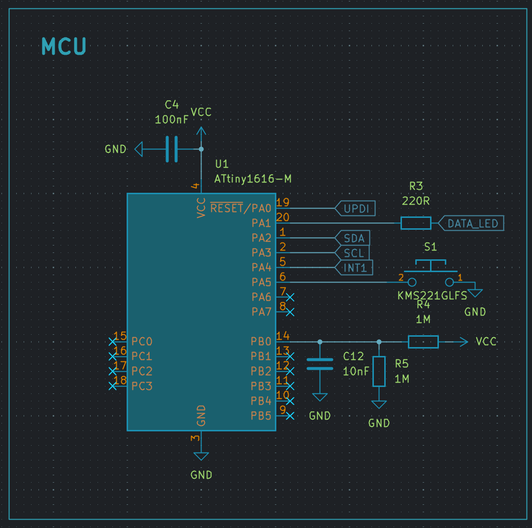
When designing a modern battery-powered gadget, choosing the right MCU is critical. I bypassed the standard ESP32 or massive ARM chips for this project. They are absolute overkill and power hogs for an application like this. Instead, I went with the ATtiny1616-M (VQFN-20 package).
Here is why this chip is a sleeper hit:
- Memory & Pins: 16 KB of Flash, 2 KB of SRAM, and up to 18 GPIOs – plenty for driving the matrix and talking to sensors.
- Low Power Execution: Active current down to microamps, and deep sleep modes that sleep soundly until a hard interrupt wakes them.
- UPDI Protocol: Single-pin programming and debugging. Look at the
UPDI Programmingblock in the schematic – it only takes VCC, GND, and one single UPDI line to flash the firmware.
2. Sensing the Roll: LIS3DH Accelerometer via I2C
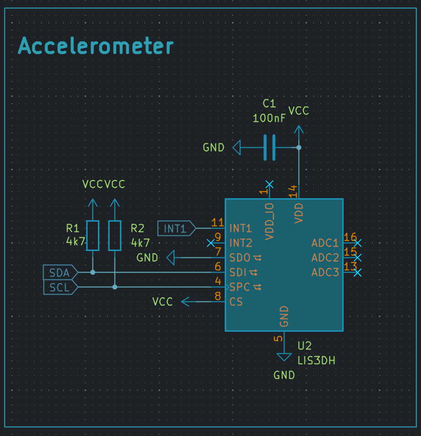
To make the dice responsive, it needs to know when it’s being shaken or thrown. I integrated the LIS3DH ultra-low-power 3-axis linear accelerometer.
- Communication: Connected strictly via hardware I2C (SDA/SCL lines) with
4k7pull-up resistors (R1,R2) pulled straight to theVCCrail. - The Magic Trick (Interrupts): To avoid constantly polling the sensor (which wastes massive battery), the LIS3DH is configured to fire a hardware interrupt on the
INT1line whenever it detects a threshold acceleration (a shake). This line is tied directly toPA5on the MCU to snap it out of deep sleep.
3. Power Architecture & Aggressive Power Saving
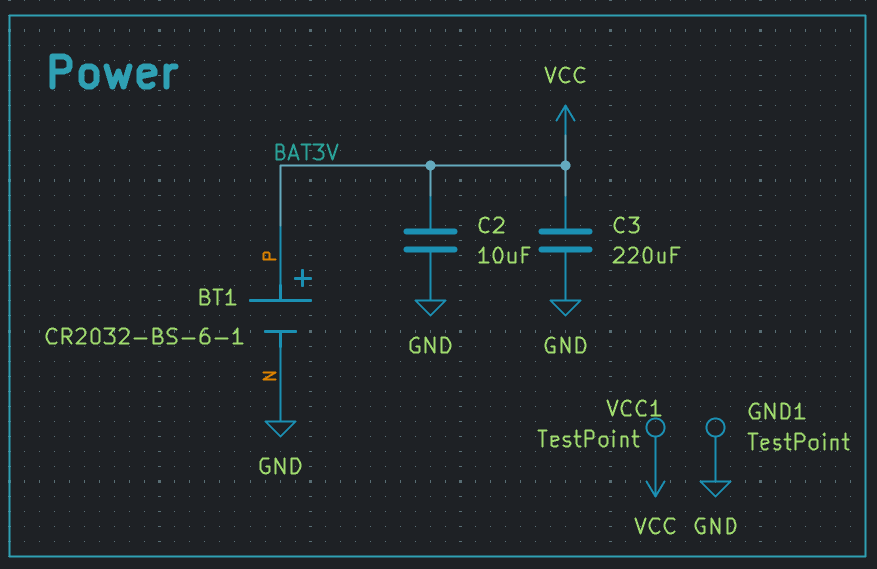
The entire device is pushed by a single CR2032 3V coin cell (BT1). Since a coin cell typically holds only around 210-240 mAh, the hardware architecture needs to be flawless:
- Decoupling Bulk: We have
10uF(C2) and220uF(C3) capacitors right at the power entry. Coin cells have high internal resistance; when the LEDs flash, those capacitors act as a structural reservoir to prevent voltage dips that could reset the MCU. - Zero-Current Idle: When the dice isn’t moving, the MCU and accelerometer stay in sleep mode. Total quiescent draw is kept to a minimum, ensuring the battery lasts for months.
4. The LED Matrix (Multiplexing Layout)
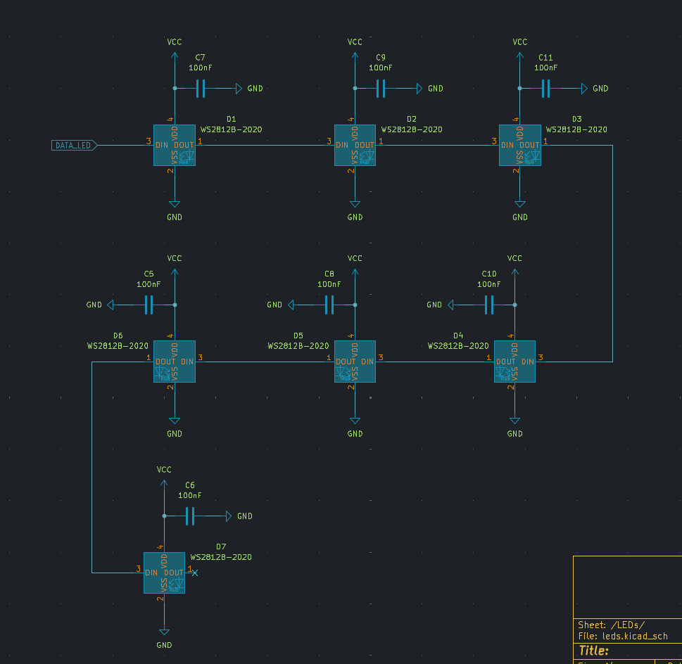
To drive 7 independent multicolor dots for the dice faces, I avoided standard passive LEDs entirely. Instead of wasting GPIOs on row/column scanning or complex charlieplexing, I integrated the ultra-miniature WS2812B-2020 addressable RGB LEDs.
Here is why this is a massive win for the e-Dice architecture:
- One Pin to Rule Them All: All 7 LEDs are daisy-chained together. The ATtiny1616 talks to the entire string using a single data pin, pushing a high-speed bitstream where each LED chops off its respective 24-bit color data and passes the rest downstream.
- True Cyberpunk Aesthetics: Since they are full RGB, we aren’t locked into static dice colors. We can code dynamic shifting animations, color-coded state indicators, and crisp flashing patterns when the dice is “rolling.”
- The Power Caveat: Every WS2812B has an internal constant-current driver that draws a tiny bit of quiescent current even when “off.” Managing this standby power is going to be our main battle in the firmware to keep the CR2032 from draining.\
5. The Hardware Safeguard: Minimalist Programming Interface
Look back at the schematic layout – you won’t find any reset or boot buttons here. They are completely unnecessary for this architecture.
Programming and debugging are handled exclusively via the UPDI programming block connected to the Conn_01x03_Socket (J1). Thanks to Microchip’s modern single-pin Unified Program and Debug Interface, we only need to break out three pins: VCC, GND, and the bidirectional UPDI data line. This keeps the board incredibly clean and allows us to flash new firmware directly from PlatformIO without any bulky programming headers.
Conclusion & Next Steps: Onto the PCB Layout!
With the schematic fully validated and every functional block locked down, the electrical foundation of project e-Dice is complete. We have:
- A highly efficient 8-bit brain managing the control loop.
- An accelerometer acting both as a hardware wake-up interrupt and a true physics-based source of entropy for our random number generator (RNG).
- A single-wire addressable RGB LED chain that gives us maximum visual freedom with minimal pin overhead.
The real challenge, however, begins now. Fitting a VQFN-20 chip, a MEMS sensor, seven WS2812B-2020 components, and a massive CR2032 battery holder onto a tiny, hand-held, cyberpunk-themed multi-layer board is a masterclass in tight routing.
In Part 2, we will open KiCAD’s PCB editor, look at component placement strategies, design the outer shape of the dice, dive into trace routing without creating an un-routable signal mess and then, sending it all to PCB fabrication.
Stay tuned!