e-Dice - Routing and reality of PCB Fabrication - Part 2
With the schematic fully locked down and validated, it was time to move from the abstract world of logical connections into the physical reality of copper, fiberglass, and solder paste.
The goal for Part 2 was clear but brutal: squeeze an MCU, an accelerometer, seven WS2812B-2020 LEDs, and a massive CR2032 battery holder onto a tiny, pocket-sized PCB without compromising the clean, cyberpunk aesthetic.
The end goal is to have dice PCB in a 3D printed body with Cyberpunk themes.
1. Defining the Form Factor & Board Constraints
Before dropping a single component, I had to establish the physical boundaries of the dice.
- Shape & Size: After some trials and errors I decided to stick with 40x40mm dimensions with 35x35mm for bolts and rounded edges.
- Layer Count Selection: 2-layer stackup was chosen for this specific routing density, it is sufficient and cheap.
- Component Placement Strategy: * Front Side: Reserved for the interactive elements (the 7 WS2812B LEDs arranged in the classic dice pattern). This decision kinda came to haunt me, because then I had to the much more challenging MCU side the “mirrored” way. Lesson learned.
- Back Side: Hidden engine room (ATtiny1616, LIS3DH, and the bulky CR2032 battery clip).
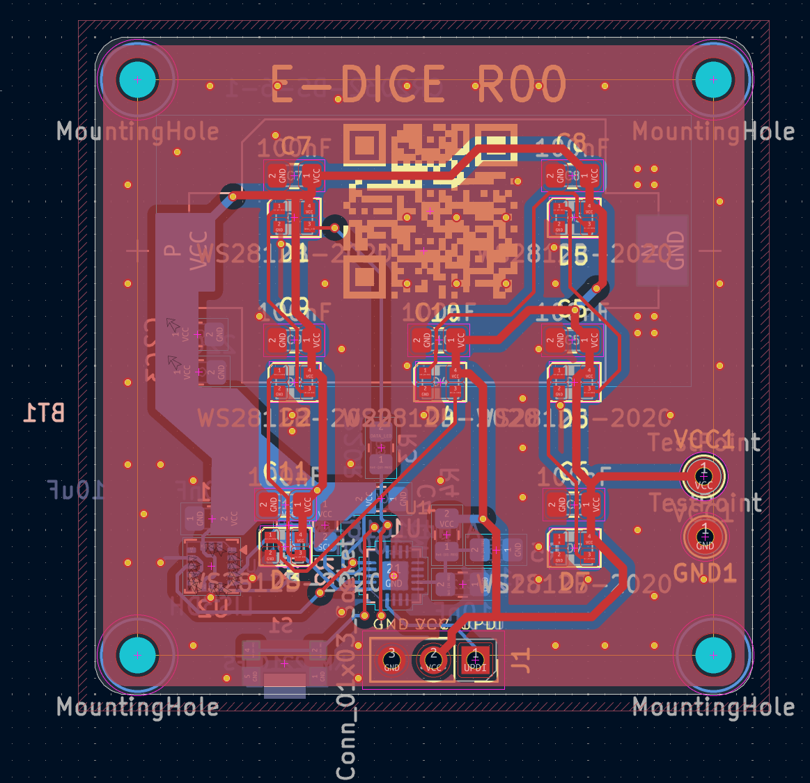
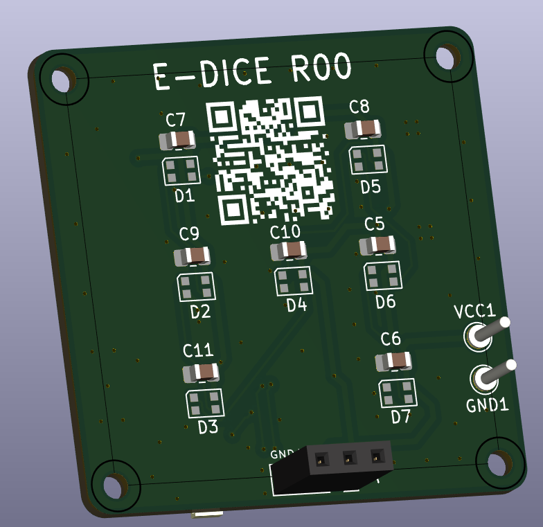
2. Routing the Ultra-Tiny WS2812B-2020 Daisy Chain
The real fun began with routing the addressable LEDs on the front layer. The 2020 package is incredibly small ($2.0 \times 2.0\text{ mm}$), leaving very little room for error.
- Single-Trace Data Flow: Tracing the $DI$ (Data In) and $DO$ (Data Out) lines sequentially from LED 1 to LED 7.
- Power Delivery: How the $VCC$ and $GND$ traces were bulked up to handle the instant current draw when all LEDs flash simultaneously.
- Decoupling Strategy: Squeezing the tiny ceramic bypass capacitors as close to the LED power pads as physically possible to suppress switching noise.
3. Squeezing the Engine Room (The Back Side)
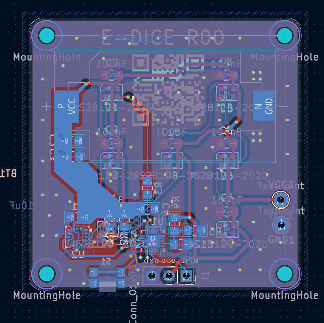
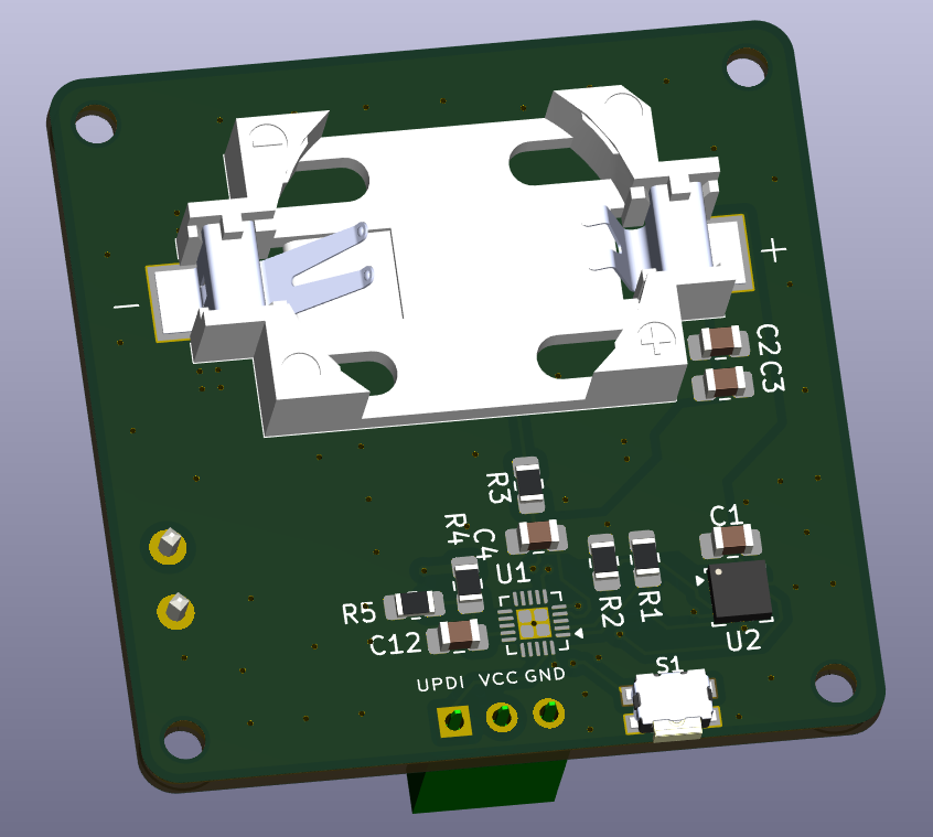
Flipping the board over, the challenge was dealing with the VQFN-20 package of the ATtiny1616 and the LGA-16 package of the LIS3DH accelerometer.
- Via Placement: Managing the escape routing from the microscopic pads of the MEMS sensor and the MCU without creating manufacturing traps.
- Keeping I2C Clean: Routing the $SDA$ and $SCL$ lines with proper clearances away from the high-speed WS2812B data line to prevent cross-talk and data corruption.
- The Battery Footprint: Adapting the back layer to fit the structural smd tabs of the coin cell holder while keeping the vias underneath insulated.
4. Manufacturing Prep & Generating the Gerbers
Leveraging the KiCAD Fabrication Toolkit
If you’ve ever manually compiled component coordinates for automated assembly, you know it’s a nightmare. For the e-Dice, using the Fabrication Toolkit plugin in KiCAD was an absolute lifesaver. Building on the friction I experienced with Zdenduino, this plugin turned generating the Gerber files, Drill data, Bill of Materials (BOM), and especially the precise Pick & Place (CPL) placement matrices into a one-click breeze.
The LCSC Component Hunting Ground
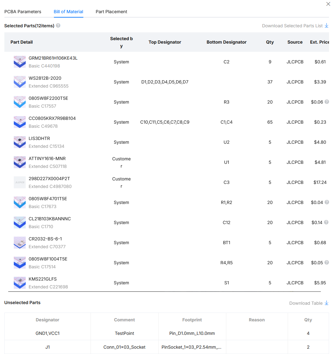
While exporting the data was easy, sourcing the parts within the JLCPCB/LCSC catalog was a tedious, brain-melting process:
- The Tactile Switch Puzzle: Finding the exact SMD footprint matching the low-profile tactile switch
SW1that would fit the compact physical clearance of the dice face. - The 17-Dollar Capacitors: Squeezing a massive $220\mu\text{F}$ capacity reservoir into a tiny 0805 package (
C3) to absorb the WS2812B voltage dips is a brutal engineering constraint. Sourcing a ceramic cap with these specs meant biting a massive financial bullet—$17 USD for just 5 pieces is wild, but necessary for stable power delivery.
The True Cost of Double-Sided SMD Assembly
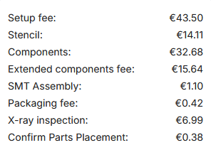
When the final invoice hit the screen, the reality of high-density prototyping sunk in: 155 Euros total. Why so expensive for a pocket toy?
- Premium Components: Rare, high-capacitance miniature caps and MEMS accelerometers drive up the raw BOM.
- Double-Sided SMT Setup: Having JLCPCB populating components on both the front (LEDs) and back (MCU, Sensor) requires two completely separate stencil setups and pick-and-place machine passes, doubling the base engineering fees.
The Final Alignment Check
Before pushing the big red payment button, the last line of defense is checking the structural placement overlays. Verifying the pin-1 orientations for the ATtiny1616 VQFN and the cathode markers on the tiny WS2812B-2020 chain is critical.
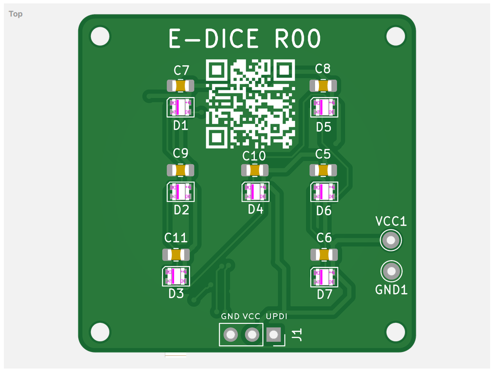
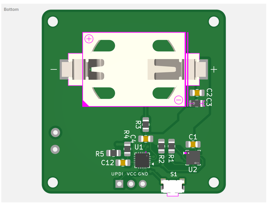
Everything aligned flawlessly. The data is sent, the factory queue is running, and the waiting game begins.
Conclusion: The Long Wait for the Mailman
The files have been uploaded, the parameters checked, and the order is officially in production. Squeezing this much functionality into such a tight footprint was an awesome puzzle to solve.
In Part 3, the packages should arrive. We will look at the physical boards and manufacturing soldering capabilities and finally flash the initial firmware to watch the e-Dice come to life for the very first time!